In this tutorial, we shall slightly deviate from our MimasV2 based projects and try to understand about how the verilog code we write gets mapped to the underlying hardware inside the FPGA.
This understanding is important when we move to more complex designs which have strict timing requirements, where tight synchronization is needed between different blocks, multiple designs are combined to obtain the end design etc. It helps in debugging, verifying and simulating such designs. Our subsequent tutorials would need this understanding.
What is a design flow? The design flow is an iterative process where the HDL code entry(or other design entry methods) is taken through a series of steps to achieve the final implementation on the FPGA which satisfies all the required specifications of the product.
You might have noticed that when you hit the ‘implement top module’ button, the process window shows various processes running in sequence. These are ‘tools'(programs) which are provided by Xilinx which perform specific functions. This is also known as a tool chain, ie where the output of one tool serves as the input for the next tool.
Before we jump into the design flow, I would like to give a brief intro to what actually lies inside a FPGA, and how our logic gets implemented in it.
FPGA architecture:
Many one line intros to FPGAs describe them as a ‘sea of gates’. It is actually more complex than that.
Here is a block diagram showing different functional blocks located at specific locations on the chip:
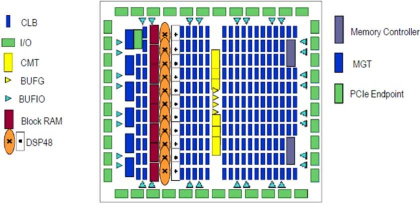
The one we will be interested in is CLB – Configurable Logic Block. You can see that they are placed in a matrix format. These are the basic building blocks of the FPGA. Here is a zoomed in version: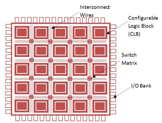
The CLBs placed in a matrix format are meshed with interconnect lines. At every node of the interconnect, a switch matrix is present – it can be used to make a connection between the interconnect lanes.
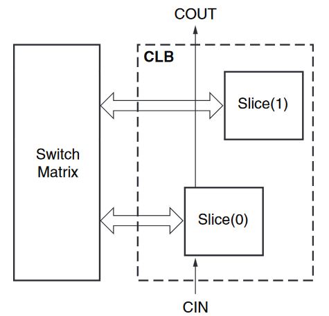
The CLBs are divided in turn into physical entities known as slices. Each CLB contains 2 slices (slice(0) and slice(1)). Slices are the ones connected to the switching matrix. There is no direct connection between slices of a CLB.
Each slice contains 4 6-LUTs and 8 FFs. The LUTs are connected to the FFs in the fashion shown below.
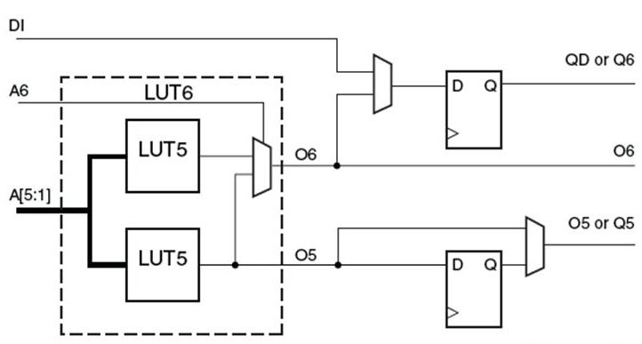
Though the CLB is more complex than this, it gives us an idea of how much a CLB can do. Each CLB contains 8 6-input LUTs and 16 flip flops. Each LUT6 can implement any 6 input logic function and the flip-flops(FFs) can be used to latch the outputs and/or feed the output back to the input to form sequential circuits such as FSMs etc.
Our finally generated .bit file programs the switch matrices to make connections between CLBs to obtain the desired circuit. Also the LUTs and Muxes inside the CLB get programmed in the process. So, it is good to think of the final design as built only with LUTs, FFs, Muxes and also some buffers and inverters.
Different FPGA families have different CLB architecture(different no. of LUTs and FFs in a CLB) in an attempt to produce more efficient implementation of any given logic.
Apart from the CLBs there are other blocks in FPGA such as DSP48 slices, which have a multiplier, adder and accumulator which facilitates implementing multipliers and MAC blocks. Thus you need not use the CLBs to implement an array multiplier, which would be also lesser in performance.
There are also CMT(Clock Management Tiles) which contains a programmable PLL to generate various clocks for the system.
There are also IO blocks which are connected to external pins. They support registering the I/O signals, pulling them HIGH/LOW internally etc.
Block RAMs(BRAMs) are dedicated memory resources, which can be used to store coefficients and data. Alternatively, note that a LUT can also function as a ROM memory. Usage of LUTs(inside CLBs) to form a memory is known as distributed memory. This wastes logic resources and also penalizes memory performance. So it should be used only when you have a reason to use the available Block RAMs for some other important job or you have run out of BRAMs.
Thus our code should get converted into designs based on LUTs, muxes, FFs, BRAMs etc which can be efficiently mapped to the FPGAs hardware. Lets now understand the design flow.
Design Flow:
Here is a broad overview of the various processes in the design flow:
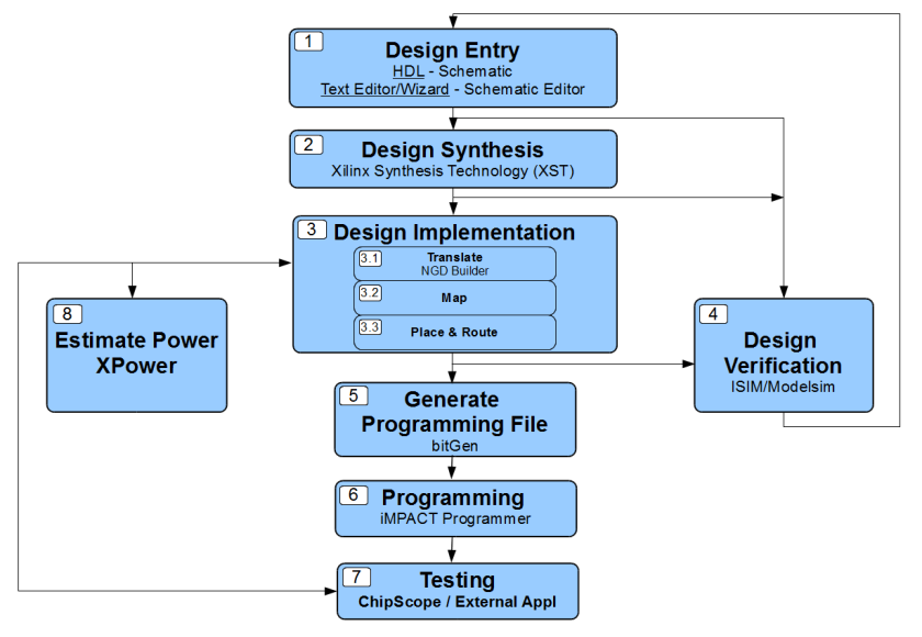
I will try to provide a clear intro to all the blocks with examples to aid understanding. Note that I will be dealing with Xilinx specific design flow. Xilinx has its own name for its tools XST, iMPACT etc and its own file extensions. But the basic framework remains same across vendors.
1) Design Entry:
The Design flow actually starts with the system specification and requirements. Based on that you start writing code as in previous tutorials. The code can be in either Verilog or VHDL. Another method known as schematic is available, but is rarely used as its too cumbersome for even mid-range designs.
This HDL entry uses an abstraction level called RTL – Register Transfer Level. Let us understand what is RTL. Any synchronous circuit can be described as a combination of combinational logic and registers. The input of a combinational logic comes from a register and the output is latched into another register. All inputs are sampled in and outputs are latched out at clock edges.

If I were to write a Verilog code which describes the above circuit:
reg [7:0] reg1,reg2,reg3;
wire [7:0] OUT1,OUT2,OUT;

assign OUT = reg3;

logic1 u1(OUT1,reg1);
logic2 u2(OUT2,reg2);

always @(posedge clk)
begin

reg1 <= IN;
reg2 <= OUT1;
reg3 <= OUT2;

end


module logic1(OUTval,INval);

output [7:0] OUTval;
input [7:0] INval;

//my combinational function

endmodule


module logic2(OUTval,INval);

output [7:0] OUTval;
input [7:0] INval;

//my combinational function

endmodule
Thus when I write this code, I think of the end functionality I desire in terms of transfer of data between registers and hence the name. It do not think in terms of gates, flip-flops, or transistors. It is a layer of abstraction wherein I do not care about how the design becomes hardware, since I find the 'flow of signals' easier to visualize.
Simply put, a synthesizable HDL code can be called a RTL code. This brings us to: what is 'synthesizable'? It means that the given code can be translated into actual hardware. For example, you might have used delays #5 , initial statements etc during simulations. But realize that such functionalities cannot be directly translated into hardware. If a 5ns delay is needed, some timer/counter has to be implemented with the available system clock – in other words the Xilinx tools won't do it for you.
The RTL code is easier to understand and simulate by the computer. I can represent a logic function by Z = X+Y. The host system uses a simple addition function to simulate the behavior of the function. But if I had described the same logic using a 8-bit adder consisting of many full-adders and half-adders, then it would take the computer lot of time to understand what the circuit is about and calculate the output corresponding to each input combination.
If I had given the entire design entry in schematic format or by using gate level primitives(like AND, OR, NOT etc libraries which Xilinx provides), then it is no longer RTL as you have directly specified the hardware. But you have the freedom to use it as well.
Thus at the end of design entry, we have a RTL code which is saved in a .v or .vhd file.
2) Design Synthesis:
The synthesis is done by a synthesis tool. There are synthesis tools available from both Xilinx as well as third party tool vendors. The one that comes along with your Xilinx ISE design suite is XST(Xilinx Synthesis Technology).
The synthesis tool’s job is to convert the HDL code into a lower level design based only on LUTs, FFs, Muxes and memory elements etc as explained before. This is known as a Netlist. Different FPGA families have different CLB architecture – thus synthesizer considers what device you are using. The synthesizer also performs optimization to implement the design in minimum area as possible(using minimum number of CLBs and Memory) but also meet the timing requirement of the design.
There almost always is a trade-off between area, speed and power. For example, a 8-bit adder might be implemented as ripple carry adder or carry look ahead adder. The later requires more logic & power but provides better speed ie, more number of additions can be performed each second. The criteria which you want to focus can be provided to the XST – area or performance. This is known as a constraint. The synthesizer accordingly chooses the final implementation.
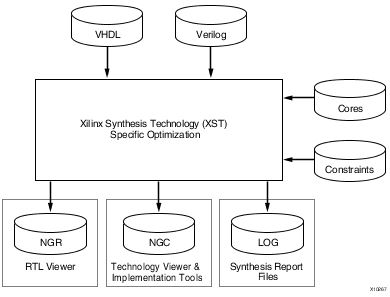
NGC: Native Generic Circuit
This diagram from Xilinx shows that the XST accepts the Verilog code and the constraints as inputs and outputs a Netlist(.ngc file). Additionally, notice that the XST also accepts ‘cores’. These cores are Netlists which have been generated by other programs or someone else which you can add to your design. These netlists contain some specific circuit of your choice. The XST ‘links’ the input netlists to the generated output netlist. Note that XST doesn’t optimize the input netlists – it simply adds them to generated netlist. But lets say the input netlist occupies a large area, then the XST makes sure the combined netlist fits into the FPGA by performing sufficient optimization on the input HDL code.
Additionally, the XST also generates a NGR file which is the RTL model of the optimized design. The RTL would contain common digital blocks such as adders, comparators, multipliers etc. This is just to let the designer verify the functionality before proceeding.
Here are some snippets of the RTL schematic and the NGC schematic of our previous audio-PWM tutorial.
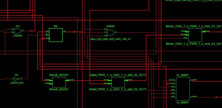
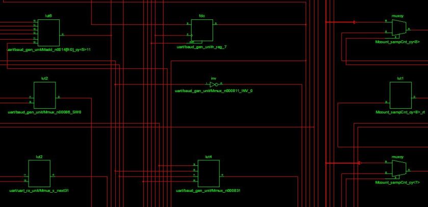
Observe that NGR contains common blocks such as mult, mux, add, gates etc. But the NGC contains only FPGA elements such as LUTs, muxes, FFs, inverters etc.
A detailed view of XST is given below:

First XST makes sure there are no syntax errors and functional errors. During HDL synthesis, XST analyzes the HDL code and attempts to infer specific design building blocks or macros (such as MUXes, RAMs, adders, and subtractors) for which it can create efficient technology implementations. To reduce the amount of inferred macros, XST performs a resource sharing check. This usually leads to a reduction of the area as well as an increase in the clock frequency. Finite State Machine (FSM) recognition is also part of the HDL synthesis step. XST recognizes FSMs independent of the modeling style(behavioral, dara flow etc) used. To create the most efficient implementation, XST uses the target optimization goal, whether area or speed, to determine which of several FSM encoding algorithms to use.
The NGC output of XST proceeds to the next process.
3) Translate:
I don’t have much to explain in the translate process. The translate process is performed by the NGDbuild tool.
The translate process basically collects all the input netlists (generated from HDL or inputted as cores) to obtain a NGD (Native Generic Database) file which contains the complete netlist information of the design. It also adds the UCF(user constraints file) which you provide.
It also performs some basic cleanup functions. For eg if you have declared a wire or register but it is not connected to anything, then translate process removes them. Overall the NGD file still contains the same netlist of FPGA elements like LUTs, FFs, muxes etc.
The output NGD file proceeds to the next process.
4) Map:
The map process is a very important process to obtain an efficient and optimal implementation of the design. The map function is performed by the MAP tool which comes along with the ISE.
The map tools are generally provided only by the FPGA vendor. This is because the map process needs to know the exact internal architecture of the FPGA to generate an optimized implementation – an information a FPGA vendor wouldn’t want anyone else to know.
We saw that the output of the synthesis/translate process contains FPGA elements connected together. These elements should be assigned their place inside slices.
The map process ‘packs’ the elements into a group so that they can fully utilize a slice(which can accommodate 4 LUTs and 8 FFs). This is not so simple as this because when signals travel from one slice to another, it introduces propagation delays. So it is desirable that elements from the same functional block be placed within the same slice or nearby slices. So there are too many combinations possible, which the mapping algorithm tries to do efficiently.
Therefore at the end of map, we know which elements will be going together in a slice. For example slice1(mux1,LUT1,LUT2,LUT3,FF1); slice2(LUT4,FF2,mux2); slice3(FF3,FF4), …..where the numbered elements are those in the netlist.
The MAP tool outputs a NCD(Native Circuit Desciption) file which also includes the timing constraints required.
The NCD file proceeds to the next process.
5) Place and Route:
The place and route function is performed by the PAR tool. Again the PAR tools are provided by the vendor itself due to the previously mentioned reasons.
Clearly, this consists of 2 individual processes – placement and routing. They are grouped together because of the similarity of jobs they perform.
At the end of map, we only know that so and so elements should go into a set of slices. Now XC6SLX9(our FPGA) contains 1430 slices. But we still haven’t decided where to place the slices in the FPGA fabric. The place function as the name states, places the slices in specific locations in the FPGA fabric. This is done taking into account the delays associated with the propagation of signals between slices and between external pins and the slices. For instance, in UART we utilize the tx and rx pins of the FPGA. It would be desirable that the RX and TX modules be placed near those pins in the fabric to achieve minimal propagation delays.
Once the slices have been placed in the fabric, we need to connect them using the switching matrix. Again this needs to be done with care to ensure that the design is not affected by excessive routing delays in the interconnects. This is done by the routing function which normally takes the longest time to complete for any design. This is again because of the sheer number of possibilities and the complexity involved. The timing requirements you specify are also taken into account.
At the end of PAR, we will have a routed NCD file which contains the complete description of the implementation.
6) bitGen:
This tool translates the description in the routed NCD file into the binary format which the FPGA hardware can be programmed with. The output is a bit file.
7) Device configuration:
Also known as programming, in this process the FPGA is configured using the bit/bin file generated previously.
How is an FPGA configured? Primarily 5 things need to be configured inside the FPGA:
- The LUTs are basically SRAM memories. 6-input LUT means its a 64 entry LUT with each entry 1 bit wide. We need to load the data into these LUTs.
- We need to decide how the LUTs are connected to the FFs. The multiplexers in between them are loaded with appropriate select line values. Also the initial states of the FFs can be loaded.
- The Block RAMs are loaded with the initial values.
- The switching matrices are also programmed.
- IOBs and other modules in the FPGA are also configured.
The FPGA we are using is a SRAM based FPGA. This means the the routing is accomplished using SRAM cells as shown below:

So, if a ‘1’ is loaded into the SRAM, then the node becomes connected else disconnected.
We know that SRAM is a volatile memory. So once power is removed the configuration is lost. For this purpose, Xilinx FPGAs provide option to automatically configure themselves from an external non volatile memory like a SPI flash chip. Fortunately, the MimasV2 has an onboard SPI flash chip(in the bottom). When you program using the .bin file you generated, the onboard PIC microcontroller receives the data through USB and writes it into the SPI flash chip. So next time you power on the board, the FPGA automatically loads the configuration from the flash (this happens when the blue LED is lit).
8) Testing:
The implemented design needs to be verified for its correctness. Actually speaking, there are simulation options which can be done at various stages of the design flow. But lets keep it for another day. The FPGA can be debugged using a JTAG probe and a host application called ChipScope.
You can view the various files such as NGC, NGD, NCD etc in the project directory. You can view the schematics under the synthesize process in the process tab. You can play around by inspecting various blocks of the schematic.
I hope that served as a helpful explanation of the design flow.
Next tutorial we will be using the Block RAM modules inside the FPGA to store audio data.
Till next time,
Anirudh
