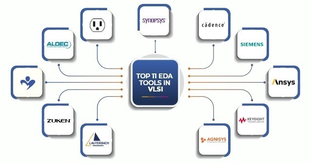
EDA TOOLS IN VLSI DESIGN
Dr.Swamynathan S M
Associate Professor/Dept.of ECE & ACOE at SNS College of Technology
#snsinstitutions #snsdesignthinkers #designthinking
Definition
Electronic Design Automation, or EDA, is a market segment consisting of software, hardware, and services with the collective goal of assisting in the definition, planning, design, implementation, verification, and subsequent manufacturing of semiconductor devices, or chips.
Technology Computer-Aided Design, (TCAD).
To design and validate the semiconductor manufacturing process to ensure it delivers the required performance and density.
Design For Manufacturability (DFM)
To verify that a design will meet all the requirements of the manufacturing process. Deficiencies in this area can cause the resultant chip to either not function or function at reduced capacity. There are also reliability risks.
Silicon Lifecycle Management or (SLM)
After the chip is manufactured, there is a growing requirement to monitor the performance of the device from post-manufacturing test to deployment in the field.
To ensure the device continues to perform as expected throughout its lifetime and to ensure the device is not tampered with.
semiconductor intellectual property or (semiconductor IP).
It provides pre-designed circuits of varying complexity that may be used as-is or adapted for a particular application. Semiconductor IP allows highly complex chips to be designed in far less time since a lot of existing design work can be reused. Due to the strong dependence of IP use and reuse on EDA tools, these markets are typically viewed as one.
How Does EDA Works?
It is primarily a software business. Very sophisticated and complex software programs function primarily in one of three ways to assist with the design and manufacture of chips:
- Simulation tools take a description of a proposed circuit and predict its behaviour before is it implemented.
- Design tools take a description of a proposed circuit function and assemble the collection of circuit elements that implement that function. This is both a logical process (assemble and connect the circuit elements) and a physical process (create the interconnected geometric shapes that will implement the circuit during manufacturing). These tools are delivered as a combination of fully automated and interactively guided capabilities.
- Verification tools examine either the logical or physical representation of the chip to determine if the resultant design is connected correctly and will deliver the required performance.
- Hardware is typically used when extremely high performance is required. This occurs when a large amount of data must be processed during simulation and verification.
- Hardware model of the circuit will perform far faster than a software program executing the same model. This dramatic increase in speed is often required to complete various tasks in reasonable amounts of time (hours to days vs. weeks to months). The two primary delivery vehicles for EDA hardware are emulation and rapid prototyping.
Assistant Project Manager, FOSSEE, IITB | M. Tech. Student IEOR, IITB
2moHow about the Open Source EDA tool, eSim developed by FOSSEE, IIT Bombay? https://esim.fossee.in/