:quality(80)/p7i.vogel.de/wcms/24/a5/24a5f4fa30af467a1a75a75f149f8c8d/0118448823.jpeg "Founded in January 2013, Caltest Instruments GmbH specializes in measuring and test equipment for AC and DC applications and offers expert advice, calibration services and rental equipment (Source: nordroden - stock.adobe.com)")
:quality(80)/p7i.vogel.de/wcms/f7/7a/f77a026e55c82dcfe853e8590719bc00/0118443413.jpeg "The vast majority of new space satellites are used in Low Earth Orbit, where the radiation environment is less extreme, the risk of catastrophic radiation-induced failure is lower. Find out more in this article. (Source: Lubos Chlubny - stock.adobe.com)")
:quality(80)/p7i.vogel.de/wcms/73/8d/738da6a85ec1b13cc0ae0c99e0a910a2/0118216103.jpeg "This article will give an in-depth insight about phototransistors. (Source: DALL · E)")
:quality(80)/p7i.vogel.de/wcms/f1/de/f1de0c5e59f67aa7f2572932ec1f4be9/0118079617.jpeg "With many features for system protection and diagnostics, the L99H92 is built for reliability and safety. Read more about this here. (Source: Tierney - stock.adobe.com)")
:quality(80)/p7i.vogel.de/wcms/b7/8c/b78cd08386fc533c603be2b832cdff84/0118481499.jpeg "At PCIM Europe 2024, ROHM will be showcasing highly efficient EcoGaN™ and SiC power solutions. (Source: ROHM)")
:quality(80)/p7i.vogel.de/wcms/4b/07/4b0752db8aad76e4001a26e692f9ec41/0118386662.jpeg "The transaction supports continuing development of high-voltage, high-power GaN technology . (Source: NAMPIX - stock.adobe.com)")
:quality(80)/p7i.vogel.de/wcms/b0/7b/b07bd3ecdebadd66e8c72e7cfe9c3102/0118335661.jpeg "Vitesco Technologies and Sanden International join forces in the pre-development of an Integrated Thermal Management System for Battery Electric Vehicles. (Source: REDPIXEL - stock.adobe.com)")
:quality(80)/p7i.vogel.de/wcms/c1/f2/c1f297688969aa72399076f01dda34bb/0118112747.jpeg "Henkel has received the Schneider Electric Sustainability Impact Award in the category ‘Large Suppliers’, featured as exemplary partner in new video series. (Source: aFotostock - stock.adobe.com)")
:quality(80)/p7i.vogel.de/wcms/ae/8a/ae8ac8d206b0b8d7bf8de4611c527549/0118332208.jpeg "Efficient: The two-layer perovskite solar cells can achieve higher efficiencies than silicon cells. Read more about this here. (Source: Empa)")
:quality(80)/p7i.vogel.de/wcms/c1/0a/c10a3236d632c46a13281af0fccaec46/0118327272.jpeg "The hallmark feature of aluminum PCBs is their exceptional thermal conductivity compared to standard PCBs. Find out more below. (Source: YouraPechkin - stock.adobe.com)")
:quality(80)/p7i.vogel.de/wcms/08/4b/084bdffffea262d1988a4a9092ac74a6/0118170678.jpeg "Could lightsabers exist in our time and age? Find out more in this article. (Source: jhathome on Pixabay)")
:quality(80)/p7i.vogel.de/wcms/df/6d/df6d4da46e35064efa91d9b8658131a0/0118004183.jpeg "RAAAM has developed the most cost-effective on-chip memory technology in the semiconductor industry, providing 50% area reduction over high-density SRAM and reduced power consumption by a factor of five. (Source: Johannes - stock.adobe.com)")
:quality(80)/p7i.vogel.de/wcms/a0/22/a0220573ab4987d56f248dd3d9712760/0117238956.jpeg "Technology Computer-Aided Design “TCAD'' is used to optimize the manufacturing process of semiconductors. (Source: Gorodenkoff - stock.adobe.com)")
:quality(80)/p7i.vogel.de/wcms/4e/13/4e1363ce48fc85e61d98a235969d4638/0116922802.jpeg "(Source: Hseyin - stock.adobe.com)")
:quality(80)/p7i.vogel.de/wcms/70/14/7014ecedef4954eb2b455e5a522804b7/0102877609.jpeg "dSPACE provides comprehensive end-to-end solutions for developing and testing e-mobility and e-drive applications – to shape and master the rapid transition to electromobility together with their customers. (Source: © dSPACE GmbH)")
:quality(80)/p7i.vogel.de/wcms/8d/a5/8da5b7876ca5418c7a6666a4b6fe01ed/0116529715.jpeg "For the first time, high-fidelity thermal simulation data can be shared in the electronic supply chain while protecting semiconductor OEM’s intellectual property. (Source: Noah - stock.adobe.com)")
SEMICONDUCTOR DESIGN VLSI design styles and tools
Related Vendors
:fill(fff,0)/p7i.vogel.de/companies/63/c7/63c7da97be945/diotec.png "diotec (Diotec Semiconductor AG)")
:fill(fff,0)/p7i.vogel.de/companies/60/7e/607ec89d5d9b5/white-frame.jpg "white frame.jpg (www.rohm.com)")
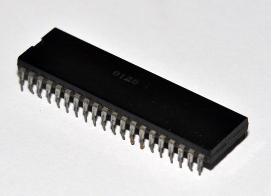
VLSI design style impacts the application of the chip, design cycle time, and cost of the project. The article explains different types of VLSI design types. As there are many VLSI design software available worldwide that are required at various stages, this article also lists a few software suites that offer hierarchical VLSI design capabilities from top to bottom.

What are VLSI design styles?
VLSI design styles are a set of different methodologies and approaches to design ICs. The design styles can be implemented either during the physical implementation of the design or in the field of the application. The article lists a few VLSI design styles below.
FPGA (Field Programmable Gate Array)
An FPGA contains an array of configurable logic blocks, input/output buffers, and programmable interconnects. There are thousands of logic gates in an FPGA that have programmable interconnects. The specialty of FPGA is the flexibility to customize and reconfigure the hardware multiple times after fabrication. This is because no physical manufacturing step is needed for FPGA customization. Hence, FPGA is a “field-programmable” IC.
The gates of MOS pass transistors are connected to the output terminals of RAM cells inside the FPGA structure. By programming the RAM cells and setting up configurable switches, an FPGA can be reprogrammed. In simple words, a hardware description language (HDL) can program, and a Boolean function can implement an FPGA VLSI design style as per the system requirements.
The advantages of FPGAs include clock frequencies up to 800 MHz, fast prototyping, fast development, customization, ease of reconfiguration, and turnaround time. Typically, a modern car contains 10-12 FPGAs.
Gate Array Design
Gate array design implementation requires two processes during the manufacturing process. After initial deep processing steps, the standard mask generates an array of uncommitted pMOS and nMOS transistors on the chip that can be customized. Secondly, there is a customization option in the process of metallization. As discussed in our article "Semiconductor circuit design: key chemical procedures", the process of embedding metal interconnects is an end procedure of the fabrication process. Programming custom metal masks can form basic logic gates in the chip.
A gate array design is a set of capabilities between a flexible FPGA and the reliability of fully custom designs. Unlike FPGAs, gate array design cannot be reconfigured after manufacturing. The customization option offers reprogrammability during the manufacturing process. Once the gate array design chip is manufactured, changes to hardware design are challenging. The advantages of gate array design are high chip utilization factor, chip speed, and short turnaround time.
Full Custom Design
In a fully custom-designed chip, each mask is designed separately and is unique. In simple words, each transistor and interconnect is designed and placed by the teams. A designer is able to design and place up to 10 transistors every day. A single-cell design is not stored in the library and is not used again. The benefit of choosing a fully custom design achieving optimal performance and control over the design.
However, it makes fully custom design costly and time-consuming. The drastic increase in design cycle time may exceed the lifetime technological window of the chip, require extensive designer time, and spoil the marketing budget. To overcome cost and time, fully custom designs for memory-based chips are designed once and reused repeatedly in multiple applications. Logic-based chips can use some portion of a fully custom design style and integrate it with other designs to form a hybrid design. New ASIC technologies are designed with a fully custom design.
:quality(80):fill(efefef,0)/p7i.vogel.de/wcms/65/95/65952af359336/ametek-whitepaper-programmable-sources-coverbild.png "Ametek Whitepaper Programmable Sources_Coverbild")
Standard Cell Design
A standard cell-based design, or poly-cell design, overcomes the limitations of high cost and design time for fully custom cell design. The standard-designed cell requires designers to develop a custom-masked cell. The difference between a standard cell-based design and a fully custom design is storage. While a fully custom design requires designing a new mask, a standard cell design develops and stores the mask in a library.
The standard pre-designed and pre-characterised library may contain logic gates like NAND, NOR, XOR, etc, along with inverters, adders, multipliers, flip-flops, and various other digital electronic components. The floor plan for standard cells places cells with a fixed height together to form a row. Several logic gates can be implemented multiple times in this design style. The logic cell has to be extracted from the library and placed in the row to interconnect with neighboring cells to attain a desirable area, speed, power, and cost.
Structured ASIC
An ASIC (Application Specific Integrated Circuit) performs in special applications rather than serving general purposes in electronic systems. For example, the 54XX family follows military applications and the 78XX is a series of voltage regulator ICs. An ASIC is only designed once. Throughout the years, sellers have kept on adding new features. A structured ASIC, on the other hand, is a hybrid between ASIC and FPGA.
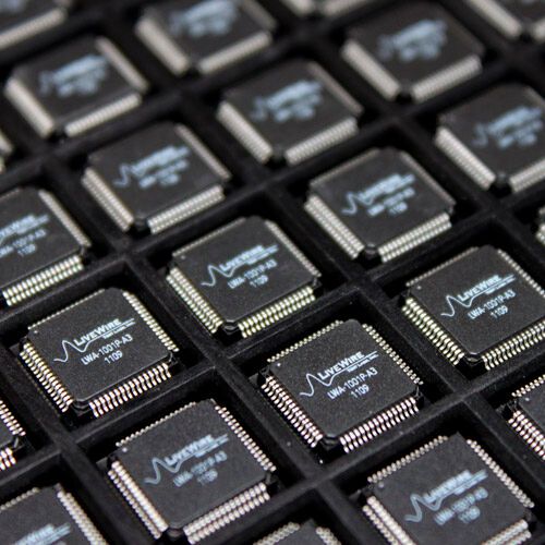
The internal characteristics of a structured ASIC are similar to an FPGA. However, a structured ASIC is not field-programmable. Similar to a standard cell, a structured ASIC contains predefined cells in the library and is mask-programmable. The lower metal layers are pre-defined during fabrication and higher layers are reconfigurable for the design. Structured ASIC has the high performance of an ASIC and low cost and turnaround time like an FPGA.
VLSI Design Tools
VLSI design tools are needed to perform tasks such as design, specifications, synthesis, simulation, floor planning, layout, placement, routing, testing, power analysis, optimization, and many other steps. The VLSI design hierarchy from top to bottom, as discussed in the previous article VLSI: Very Large Scale Integration, requires multiple software.
VLSI design isn’t one person’s game but an engineering team’s combined effort. Each point in the design hierarchy requires multiple designers and software suites. Even at a single stage of algorithm design, a software suite is required to perform all the necessary functions. VLSI design software starts digital design from scratch and leads up to physical mask generation for fabrication. For example, software defining the target’s chip architecture is not capable of routing, logic cell placement, or floorplanning.
Moreover, VLSI design requires complex programming language- hardware description languages (HDL) like Verilog, SystemVerilog, and VHDL. There are many VLSI design tools in the market. Some companies tend to gain access to an entire suite of VLSI software from a single vendor. However, most companies use software from multiple vendors according to system requirements and project life cycles.
As there are N VLSI design software, the article discusses popular software suites from SaaS companies in semiconductor design and manufacturing.
:quality(80):fill(efefef,0)/p7i.vogel.de/wcms/65/5c/655c87f111972/202311-whitepaper-tektronix-coverbild.png "202311_Whitepaper Tektronix_Coverbild")
ANSYS
Ansys, Inc. is an American multinational company headquartered in Canonsburg, Pennsylvania. The company offers multiphysics software to product teams and engineers for design and finite element analysis. For VLSI design, Ansys tools offer high-speed software for the smallest transistor technologies like FinFET and GAA. The multiphysics software also involves thermal, electrothermal, and electromagnetic aspects of the design. Some of Ansys's software for VLSI design- semiconductors (SC) are RedHawk-SC, RedHawk-SC Electrothermal, Totem-SC, PathFinder, PowerArtist, VeloceRF, etc.
SYNOPSYS
Synopsys is an American company headquartered in Sunnyvale, California. For the last 37 years, Synopsys has been a consistent name in the semiconductor design and manufacturing industry. Synopsys offers many EDA tools including silicon design tools to develop efficient hardware. There is proprietary software from the company to manage the silicon chip life cycle. Some of the widely used tools from Synopsys are Design Compiler, Fusion Design Platform, Verification Continuum, Silicon Engineering Platform, and Silicon Lifecycle Management Platform.
Siemens EDA
Siemens is originally a German multi-industry company. The SaaS providing unit from the parent company owns EDA tools under Siemens Digital Industries Software based in America. In 2017, the popular software Mentor Graphics was acquired by Siemens and is now selling software tools under the name of Siemens EDA. Siemens EDA tools design, synthesize, verify, floor plan, and generate physical design masks for various modern ICs. Softwares include Aprisa for digital IC implementation, mPower for power integrity analysis, Oasys-RTL for Logic synthesis, Precision for FPGA synthesis, and PowerPro for power optimization.
Cadence
Cadence Design Systems is an American multinational company headquartered in San Jose, California. Cadence has a wide portfolio of EDA tools ranging from circuit simulation, PCB design, and hardware-level coding to VLSI design. Some software from Cadence are Genus Synthesis Solutions, Tempus Timing Solution for FinFET, Innovus Implementation System, Voltus IC Power Integrity Solution, Stratus, Virtuoso Layout Suite, Protium Enterprise Prototyping for SoC, and many more. Cadence Allegro is another popular tool to work with PCBs.
Keysight Technologies
Keysight Technologies is an American company headquartered in Santa Rosa, California. The company has been known for a long time to offer electronic test equipment and software. For VLSI design, Keysight Technologies tools offer software named PathWave Advanced Design System (ADS) for circuit design and simulation at the system level. The software performs high-speed digital design and tests for making efficient power converter designs, and RF components that are free of unnecessary parasitic capacities and mixed-signal barriers.
Power Electronics in the Energy Transition

The parameters for energy transition and climate protection solutions span education, research, industry, and society. In the new episode of "Sound On. Power On.", Frank Osterwald of the Society for Energy and Climate Protection Schleswig‐Holstein talks about the holistic guidance his organization can provide.
Listen now!
(ID:49936948)
:quality(80)/p7i.vogel.de/wcms/a7/f0/a7f002f0bd25624580f49d6c45ea2787/0115772357.jpeg "The article details the same process that makes it possible: VLSI! (Source: Jack Soldano - stock.adobe.com)")
:quality(80)/p7i.vogel.de/wcms/9d/e0/9de0c6f0fcd9f328c533d415a3c4488e/0113286401.jpeg "The article explores the levels of coding for electrical/electronics engineers and lists such top 5 programming languages. (Source: Jamie - stock.adobe.com)")